
Research themes
Our research is focused on solving the challenges we face today and is grouped into five different themes that overlap and support each other.
Covering topics as broad as advanced functional materials and robotics for extreme environments, our research takes advantage of the University's modern facilities - as well as our collaborations with centres and institutes - to produce truly outstanding work.
Explore each of the themes and the areas in which our staff specialise below.
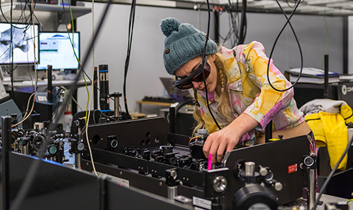
Advanced functional materials and devices
Applied research, ranging from atomic-level to devices leading to new technology development.

Electronic engineering for agriculture
Research into the many different uses of electronics in agriculture technologies.

Power and energy systems
The production, transmission and use of electrical energy in the 21st century.
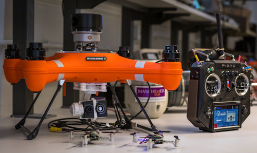
Robotics for extreme environments
Robotic systems development to explore and manipulate objects in extreme environments.

AI at Manchester
It began here, with Turing’s seminal paper on AI. Today, we’re designing AI that tackles global challenges and transforms lives.
Learn more about AI at Manchester
Areas of expertise
Our Department's researchers specialise in a number of areas of expertise, applicable to all of our core themes.
Read more