Photon Science Institute
The Photon Science Institute (PSI) was established in 2005 to bring together experts from a range of fields to foster interdisciplinary collaborations and to maximise the potential applications of photon science.
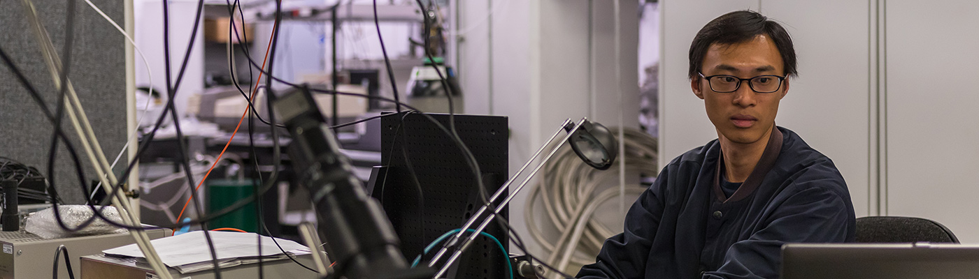
The initial development phase of the PSI involved a £50 million investment in world-class research infrastructure, including more than £20 million of high-spec laser, spectroscopy and imaging equipment. The activities and facilities supported by the Department and our academics now include the provision of leading photon science facilities that span from the THz through mid IR to UV and X-ray energies, and which are delivered with CW to femtosecond timing.
The Department's members have further extended these facilities to include modern electronic test and measurement capability, delivered in conjunction with high magnetic field (7T) and low temperature (1.4K) environments. The provision of ultra-stable nanoscale characterisation has been added to these, along with the unique ability to modify materials on the atomic scale using direct-write ion-beam technologies.
Today the PSI continues to evolve and enables outstanding science and engineering to be delivered by our researchers. The Department has provided leadership for both the PSI and the Henry Royce Institute - the UK's National Institute for Advanced Materials - whose hub is presently based within the PSI. The capabilities and facilities highlighted below are those delivered by academics within the Department and are complemented by the significant other capability offered within the PSI.
Capabilities
Optical spectroscopy
- X-ray to THz photon sources and detection capability providing comprehensive spectral coverage
- ~20fs through to ps, 1KHz to 80MHz source (eg Coherent HELIOS, Spitfire-HPR, Legend Elite-USP Duo, Micra-CEP, Mira-OPO, Mantis Spectra Physics Mai Tai HP)
- Steady-state, frequency and time domain optical characterisation (eg PL, PLE, FRS, DLTS, Raman, FTIR, Abs, etc)
Electronic test and measurement
- Fully-specified semiconductor parameter analysers (eg Keysight B1500; Keithley 4200 systems)
- Semi-automated semiconductor wafer probe-station
- EM-shielded laboratories and facilities for low-noise high-sensitivity characterisation
- Photothermal materials characterisation (eg photo-Seebeck)
Materials modification and device fabrication
- Platform for Nanoscale Advanced Materials Engineering (P-NAME) enabling direct ion-writing
- Inert atmosphere solution processing and deposition for rapid device prototyping
- X-ray to THz photodetector device characterisation
- AM1.5 solar simulator for photovoltaic device characterisation
- Waveguide and integrated chip device development
Test facilities
Advanced Electronic and Photonic Materials Device Testing Facility
This facility brings together:
- Comprehensive optical sources
- Cryogenic (down to ~1.4K) to high (~800K) temperature sample and device measurement
- High magnetic field (7T) wide-bore superconducting magnet integrated with photonic and electronic characterisation
- Montana Instruments nanoscale workstation for the study of low-dimensional materials and devices
EPSRC-supported facilities
The PSI also houses the following Engineering and Physical Sciences Research Council (EPSRC) supported facilities, which complement those directly supported by the Department:
- The National Electron Paramagnetic Resonance (EPR) Facility
- The Henry Moseley X-ray characterisation and tomography facility
- The X-ray Photoelectron Spectroscopy (XPS) facility