Advanced functional materials and devices
Fundamental and applied research spanning atoms to devices leading to new technology development.
Key researchers
Electronic and photonic technologies have revolutionised our world and now underpin all areas of modern life.
Our research aims to ensure that future advanced technologies continue to emerge that provide solutions to existing and future global challenges.
The breadth of our research includes new materials and devices for optoelectronics, electronics and memory, a wide variety of sensing technologies, small-scale power generation and for quantum technologies.
Functional materials
We have active research programs in 0D (quantum dot), 1D (quantum wires), 2D (eg graphene) and nanocrystalline and bulk (crystalline and amorphous) semiconductor materials. We use doping to provide additional functionality to these, enabling enhanced interaction with light, electrons and magnetic fields.
Our research has overcome a search lasting over 50 years for a method of creating n-type chalcogenide materials through our developing of non-equilibrium doping. We are now developing this concept through an EPSRC-funded collaboration in order to provide new material solutions to enhancing key technologies that utilise these materials, such as phase-change memory and non-linear photonic devices.
The development of colloidal semiconductor nanocrystals has been dramatic, with their use being quickly adopted in commercial products such as high-resolution televisions. We are working to replace heavy-metal based systems with nitride-based nanocrystals, while also extending their efficient operation into the near-infrared spectral region and adding magnetic functionality via an EPSRC-funded collaboration.
We are investigating the co-integration of 0D, 1D and 2D-materials with the established silicon platform and other systems to overcome existing bottlenecks and enhance and create novel functionalities. Combining multi-dimensional structures is a promising route to make use of the unique properties of these new materials, while ensuring scalability.
Healthcare technologies
As part of the Global Challenges Research Fund, our aim is to develop a low-cost miniaturised, integrated chip-based optical coherence tomography (OCT)-based healthcare diagnostic tool, which will provide a transformative change to the level access to clinical imaging technology in countries on the OECD Development Assistance Committee list.
The development of new healthcare technologies is an important part of our mission to create impact. The Global Challenges Research Fund (GCRF) is a five-year, £1.5 billion fund that is a key component in the delivery of the UK Aid Strategy. Through this we are working with partners in the UK at Glasgow, in the US at the Harvard Medical School and within Nepal to develop photonic imaging technologies. Our vision is to develop a low-complexity, low-cost, miniature OCT system incorporated within existing bronchoscopy or catheter based medical devices that could be used along with commercially available data acquisition hardware and analytical software on a mobile platform. Such a system can provide the necessary access to a sophisticated imaging diagnostic tool that could displace basic spirometry and even fibre based bronchoscopy as the gold standard for early diagnosis of chronic obstructive pulmonary disease (COPD).
We have ongoing computational and experimental activities, studying and enhancing X-ray interaction in novel and nanocrystal materials. These are being explored with the aim of developing X-ray detection and imaging technologies with improved sensitivity and/or low cost technologies. This work complements the ongoing development and use of X-ray sources as diagnostic and treatment tools in healthcare environments.
Nanoscale engineering
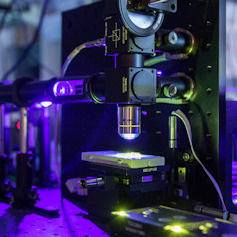
This research is establishing a Platform for Nanoscale Advanced Materials Engineering (P-NAME) facility, incorporating a new £2m tool that provides the capability to fundamentally change our ability to design and engineer materials on the nanoscale. It will be established within the Henry Royce Institute at The University of Manchester within the Photon Science Institute.
Modern technologies based on the electronic, optical and magnetic properties of materials are built upon the ability to engineer these to suit a particular functional need. As technology has developed, this need has extended to include multifunctionality at multiple length scales, placing increasing demand on the level of advanced materials engineering that is required.
With the development of nanoscale materials and devices, the ability to perform this type of engineering has become compromised by the techniques and capability that are available, and their suitability for use in manufacture.
We are developing the experimental capability required to directly address this serious capability gap through delivering the P-NAME facility. P-NAME will enable the electronic, optical and magnetic doping of advanced materials to provide localised control of functionality, with sub 20nm precision. The development of P-NAME will provide internationally leading capability, enhancing the UK's ability to deliver advanced materials research.
Photonic devices
Our research is improving existing technologies, such as lasers and photovoltaics, by advancing understanding of current device limitations and engineering solutions to overcome these. We are also pioneering the development of new integrated technologies for photonic systems, which include memory devices.
The Manchester group has a 40-plus year history of studying the properties and defect chemistry in LED and laser materials. Recent work has focused on the effect of defects on materials for Photovoltaic (PV) cells and low energy lighting.
Our work on PV cells focuses on working with major solar silicon manufacturers to identify elements and their complexes that limit the efficiency of cheap mass produced solar silicon. The principle technique used is deep level transient spectroscopy combined with SIMs, microscopy, IR absorption and other techniques to find and identify recombination centres in solar silicon provided by collaborators. Our feedback is used to adjust the composition of feedstock and inform process flows so as to optimise cell performance; this is funded by an EPSRC award from the Supergen programme and is a collaboration with the Universities of Oxford and Warwick.
Nitride-based semiconductor devices are one of the major technological success stories of the last 20 years. They are behind the sudden growth in cheap high-efficiency LED lighting and are also starting to become the technology of choice in high power switching applications. By dominating these two markets, this one material has the potential to reduce by up to 20% the electricity demand of the planet. The defects chemistry of the nitrides is an entirely new field and the Manchester group has recently received substantial EPSRC funding to begin applying its expertise to the study of the role of defects in limiting the performance of nitride LEDs and transistors. This project will involve the development and commercialisation of an entirely new form of deep level transient spectroscopy for the task.
One of our principle research themes is in silicon photonics; here we are developing novel waveguide based micro-ring resonator and interferometer devices for fast optical switching and modulation for telecommunications applications. We are also combining novel techniques for improved dopant activation with strain engineering in Ge/SiGe materials for applications in CMOS compatible solid state laser and MOSFET devices. Our fundamental materials research activities in this area include studying the formation and electronic doping of silicon nanostructures and the atomic-scale processes leading to efficient light emission in rare-earth based phosphors for future nano-optoelectronics.
Quantum technologies
We are leading the development of a key tool for enabling solid-state quantum technologies in collaboration with partners at the University of Surrey. The single ion multispecies positioning at low energy (SIMPLE) tool will enable deterministic doping of key ion species with sub-20nm spatial precision, realising rapidly scalable qubit arrays.
Funded through an EPSRC award of around £3 million, the development of this capability will enable the doping of diamond, silicon and other semiconductors with single atoms in order to create qubits. The SIMPLE tool commissioned to achieve this enables isotopically selected ion species (eg N, P, Si, Er, Bi) to be implanted with sub-20nm precision. The tool will is housed within the UK National Ion Beam Centre (UKNIBC), and EPSRC mid-range facility, at the University of Surrey site.
Sensing devices
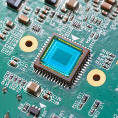
We have developed high-performance photodetectors and cover the ultraviolet to mid-infrared spectral region. We are also undertaking research into next-generation X-ray detectors and magnetic field sensing devices. Our devices are able to sense a wide variety of physical effects such as strain, temperature and pressure.
Our sensing devices cover the range from electronic over nano-/micro-electro-mechanical-systems to photonic devices. Various physical principles are exploited to allow our devices to interact with the environment and detect electromagnetic radiation over a broad wavelength range, strain, temperature and chemical species. An example is in the remote detection of the human pulse based on light detection without the need for direct contact of the sensor to the human body, based on high-detectivity graphene-silicon photodetectors.
We are developing novel optical sensing devices, based on 2D materials (graphene/graphene oxide) integration with the established silicon photonics platform to realise enhanced performance in molecular sensing in the liquid and gas phase. This work is currently supported by a King Saud University/The University of Manchester research partnership and we are also working with collaborators on mid-IR devices for the targeted detection of specific gases.
Our recent work on hybrid nanocrystal photodetectors has led to the development of ultra-high performance devices, which extend the spectral range covered by a single device from the ultraviolet through to the near infrared while matching the performance of commercial detector systems. The potential of nanocrystal systems is now widely accepted, and new avenues are being explored to extend their use to X-ray detection and the direct detection of magnetic fields.

Areas of expertise
-

Electrical materials
Our research covers everything from superconducting materials to using graphene to create 2D materials.
Read more
-
Electronic devices
Our work spans the modelling and synthesis of atomic layer thin films using Molecular Beam Epitaxy.
Read more
-
Photonics
Our researchers work across all areas of photonics, including the development of new advanced materials.
Read more